


Quick Entry
Submission Reviewer Office Work Editor-in-chief
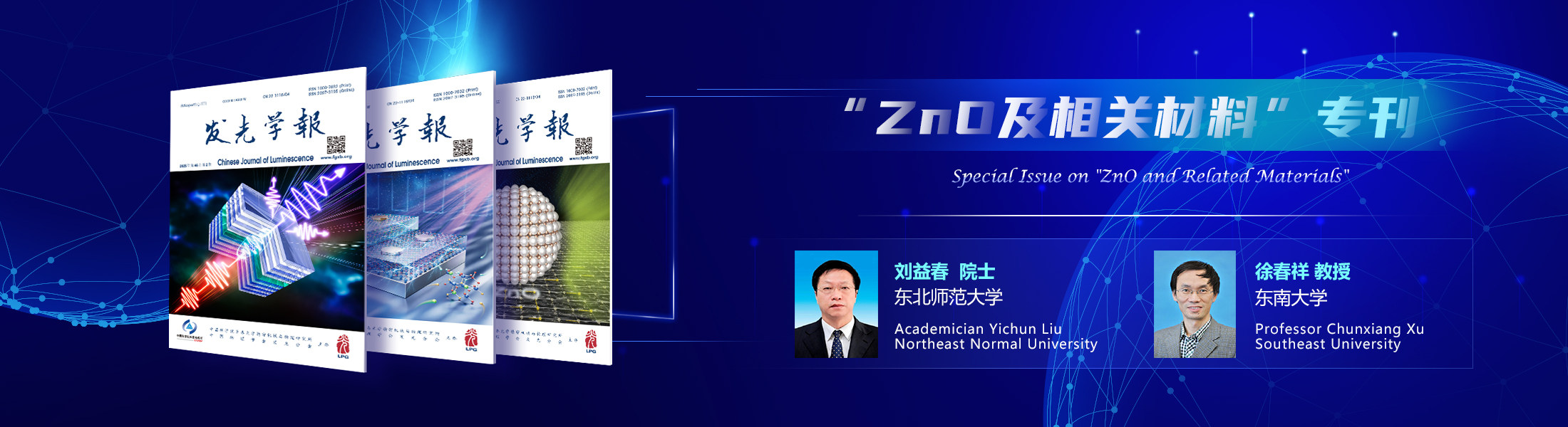
Chinese Journal of Luminescence

- Editor-in-Chief:Fengyi Jiang
- ISSN:1000-7032
- eISSN:2097-3195
- CN:22-1116/O4
- Supervisor:Chinese Academy of Sciences
- Sponsor:Changchun Institute of Optics, Fine Mechanics and Physics, Chinese Academy of Sciences, Luminescence Branch of Chinese Physical Society, State Key Laboratory of Luminescence and Applications
- Publication frequency:Monthly
- Tel.:0431-86176862
- E-mail:fgxbt@126.com
- Address:No.3888 Dong Nanhu Road, Changchun, Jilin, China
- Announcement of 5th International Conference on Mechanoluminescence and Novel Structural Health Diagnosis(ML-s)
- International Conference on Optoelectronic Materials, Technology and Application 2022
- The 9th National Conference on Luminescent Properties of Doped Nanomaterials
- 20th International Conference on Luminescence
- International Academic Frontier Forum on Luminescent Materials 2022
- The Second Round Announcement of Phosphor Safari 2022
- The First Round Announcement of Phosphor Safari 2022,July 30- August 3, 2022, Lanzhou, China
Rankings  更多
更多
- 0 1 Advances in Relationship Between Lattice Defects and Luminescent Characteristics 6401
- 0 2 Research Progresses of Photoluminescence and Application for Emerging Zero-dimensional Metal Halides Luminescence Materials 6164
- 0 3 Advances in Valence State Analysis of Manganese in Mn4+-activated Red Phosphors for White LEDs 5547
- 0 4 Research Progress on Structure Design of Direct Halogen Perovskite X-ray Detectors 4916
- 0 5 Basic Knowledge for Understanding Spectroscopic Property of Mn4+ Ion 4751
- 0 6 Reversible Fluorescence Modulation and Applications Based on Chromic Effect in Inorganic Rare-earth Luminescent Materials 4594
- 0 7 Enhanced Electroluminescence Properties of Tin-based Perovskites by Vitamin C Additives 4568
- 0 8 Strengthening Carrier Transmission to Achieve High Brightness and High Efficiency of Perovskite Quantum Dot Light Emitting Diodes 4227
- 0 9 Rare Earth Ion Doped Perovskite Nanocrystals 3993
- 10 Research Progress on Optical Quenching of Ce3+- and Eu2+-doped Luminescent Materials 3903
查看更多
Links
- Academic examination of manuscripts
- Light: Science & Applications
- Light: Advanced Manufacturing
- eLight
- Chinese Optics
- Optics and Precision Engineering
- Chinese Journal of Liquid Crystals and Displays
- Light Publishing Group
- Changchun Institute of Optics, Fine Mechanics and Physics, Chinese Academy of Sciences
- Latest Articles
- Cover Story
- Online First
- Archive
- Themed Collections
- Special Issue
2026年第47卷第4期
Cover Story
摘要:Color-tunable organic light-emitting devices (OLEDs) hold significant application potential in dynamic displays, anti-counterfeiting, and information encryption. In this work, a tandem-structured red-green color-tunable OLED is constructed using Bphen∶Mg as the n-doped charge generation layer (CGL). The effects of Mg and Ag doping on carrier injection and recombination behavior in the CGL are systematically investigated. Although Mg doping results in a lower current density, it yields a higher external quantum efficiency (16.9%), which is more favorable for efficient luminescence. By adjusting the stacking order of the red and green emitting layers, the device with a green-bottom/red-top configuration exhibits pronounced voltage-dependent color tunability. Its CIE coordinates shift from (0.61, 0.39) at 7 V to (0.47, 0.48) at 19 V, a change that extends beyond the five-step MacAdam ellipse range, ensuring good visual discernibility. Based on this structure, a patterned anti-counterfeiting label is further fabricated, demonstrating dynamic switching between a red pattern at low voltage and a yellow-green background at high voltage, thereby verifying its feasibility for multi-level visual anti-counterfeiting and information encryption. This study provides experimental support for the design and anti-counterfeiting applications of high-performance color-tunable tandem OLEDs.关键词:tandem organic light-emitting device (OLED);Mg-doped charge generation layer;color-tunable;Voltage modulation;Patterned anti-counterfeiting label;Information encryption1180|611|0更新时间:2026-04-22Research Highlight
摘要:Flexible mechanoluminescent (ML) materials hold significant promise for applications in wearable optoelectronics and intelligent sensing. However, conventional materials are largely limited to visible and near-infrared emissions and often require pre-irradiation activation, which restricts their operational stability in complex environments. Recently, Lv et al. reported a pioneering development of a solar-blind deep-ultraviolet (UVC) ML elastomer (Sr3(BO3)2∶Pr3+/PDMS) driven by interfacial triboelectrification. This material integrates self-powering and self-recovery capabilities with exceptional cyclic stability. Without the necessity of pre-irradiation, the elastomer emits solar-blind UVC light peaked at 272 nm upon mechanical stimulation. The elastomer film exhibits excellent optical stability over 10 000 stretching cycles, and its luminescence intensity can recover to 90.2% of the initial value after a 24-hour resting period. This work not only extends the spectral range of ML into the solar-blind ultraviolet region but also provides new strategies for background-free optical tagging and self-powered microbial sterilization applications.关键词:mechanoluminescence;UVC emission;triboelectric effect;self-recovery;flexible elastomers1139|457|0更新时间:2026-04-22Invited Paper
摘要:X-ray imaging plays a vital role in nuclear medical diagnostics, industrial non-destructive inspection, and security inspection, where high-performance scintillators serve as the core materials for efficient X-ray detection and imaging. Developing new scintillator crystals that combine high absorption efficiency, high light yield, fast decay time, and low detection limit is a key challenge for improving imaging quality and reducing radiation dose. In this work, Cs3Lu2Cl9 crystals doped with various Ce3+ concentrations were successfully prepared by the Bridgeman method, and their photoluminescence and scintillation properties were systematically investigated. The undoped crystal exhibits intrinsic broad-band luminescence originating from self-trapped excitons (STE). Ce3+ doping significantly enhances the X-ray excited luminescence intensity. Among them, the Cs3Lu2Cl9∶5%Ce crystal exhibits the best overall scintillation performance. It shows a radioluminescence (RL) emission peak at 425 nm and achieves a steady-state X-ray light yield of 20 700 photons·MeV-1, which is seven times higher than that of the undoped sample. Its scintillation decay time is 36.5 ns. Furthermore, this crystal achieves a low X-ray detection limit of 152 nGyair·s-1 and a high spatial resolution of 14.5 lp·mm-1. This work elucidates the mechanism by which Ce3+ synergistically enhances STE luminescence efficiency in Cs3Lu2Cl9, achieved by suppressing non-radiative recombination and facilitating energy transfer. It thus confirms the great potential of Cs3Lu2Cl9∶5%Ce as a high-performance, fast-response X-ray scintillator for low-dose, high-resolution imaging applications.关键词:scintillation crystal;Bridgman method;Cs3Lu2Cl9;Ce³⁺ doping;X-ray imaging1055|431|0更新时间:2026-04-22Invited Review
摘要:Fe3+-doped near-infrared luminescent materials have drawn increasing attention due to their tunable broadband emission, excellent biocompatibility and low toxicity, demonstrating promising applications in bioimaging and nondestructive testing. Understanding the structure-property relationship between crystal structure and luminescence performance, along with optimization strategies, is crucial for developing novel high-efficiency Fe3+-doped materials. This review summarizes recent advances in Fe3+-doped NIR luminescent materials. Using Tanabe-Sugano diagrams, we analyze the luminescence mechanisms of Fe3+ in both octahedral and tetrahedral coordination environments. A systematic comparison of materials reported in the past five years is presented, focusing on their luminescence properties, optimization approaches and application fields. Finally, we discuss current challenges and future prospects to provide valuable insights for understanding emission mechanisms and developing high-performance Fe3+-doped NIR luminescent materials.关键词:near-infrared luminescence;Fe3+ doping;crystal structure;Luminescent performance Optimization strategy1638|627|0更新时间:2026-04-22

查看更多
- Featured Album

- Address:No.3888 Dong Nanhu Road, Changchun, Jilin, China Postal code:130033
- Tel:0431-86176862 Email:fgxbt@126.com
- Technical support is provided by Beijing Founder electronics co., LTD 吉ICP备11002662号-17
 京公网安备11010802024621
 - It is recommended to read the content of this site in Chrome&IE9+. Please switch to extreme mode in browser 360.
- Cookies We use cookies to help provide and enhance our service and tailor content. By continuing, you agree to the use of cookies.

0